[굿썸] Lane Margining at Receiver
아래 문서는 [PCI Express Base Specification Revision 5.0 Version 1.0 , 22 May 2019] 기준으로 작성 되었습니다.
Lane Margining at Recevier 는 PCIe 4.0 부터(16.0 GT/s 이상의 데이터 속도를 지원하는 포트에만) 적용되기 시작한 기능입니다. PCIe component 들 사이의 link 의 signial margin 을 측정할 수 있는 매우 효과 적인 방법입니다.
Margining 테스트가 완료 되면 하당 PCIe Lane의 eye diagram 과 비슷한 데이터를 얻을 수 있습니다.

아래와 같이 PCIe 디바이스들이 연결되어 있다고 가정해 보겠습니다.
CPU는
1. CPU 와 RC의 downstream port 사이의 링크 마진을 측정할 수 있습니다. (가장 짧은 path)
2. CPU 와 Retimer 의 upstream port 사이의 링크 마진을 측정할 수 있습니다.
3. CPU 와 Retimer 의 downstream port 사이의 링크 마진을 측정할 수 있습니다.
4. CPU 와 EndPoint 디바이스의 upstream port 사이의 링크 마진을 측정할 수 있습니다. (가장 긴 path)

이어지는 내용은 CPU 와 EndPoint 사이에 signal margin 을 측정한다고 가정하고 진행하겠습니다.
Lane Margining at Receiver 는 둘 사이의 link 가 L0 상태일때만 진행됩니다.
Lane Margining 은 Timing 과 Voltage 를 변경하면서 진행할 수 있는데, Timing Margining 은 필수이며, Voltage Marginig은 옵션 입니다.

소프트웨어는 Lane Margining Lane Control Register와 Margining Lane Status Register를 각 포트(다운스트림 또는 업스트림)에서 사용하여 Margin Command를 전송하고 포트와 관련된 수신기의 상태 및 마진 상태 정보를 얻습니다.
이와 관련된 Register 는 Lane Margining at the Receiver Extended Capability 입니다.
각 PCIe 포튼느 자신의 Configuration Space 에 한개씩 Margining Extended Capability 레지스터를 가지고 있습니다.
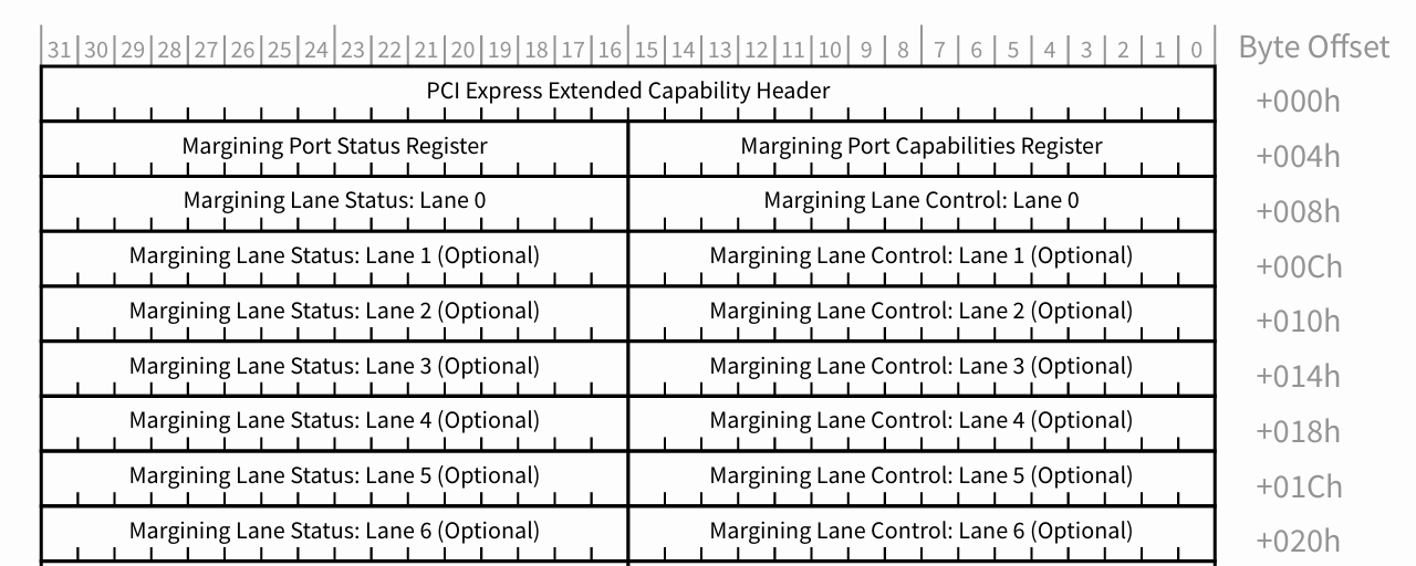
Margining Extended Capability 레지스터는 아래와 같이 구성되어 있습니다.
....

Offset 00h 에는 PCI Express Extended Capability Heder (32bits) 가 한개 존재하며, 아래와 같이 3 부분으로 나뉘어 있습니다.

Offset 04h 에는 Margining Port Capabilities Register (16bits) 가 한개 존재하며, 아래와 같이 한 가지의 내용만 담고 있습니다.

Offset 06h 에는 Margining Port Status Register (16bits) 가 한개 존재하며, 아래와 같이 2 부분의 내용을 담고 있습니다.

Offset 08h 부터는 Lane 0 에 대한 Margining Lane Control Register(16bits) 가 존재하며,
Offset 0Ah 부터는 Lane 0 에 대한 Margining Lane Status Register(16bits) 가 존재합니다.
현재 PCIe port가 총 몇개의 Lane을 보유하고 있느냐에 따라, 그 뒤에 따라오는 Lane 1, Lane 2 에대한 control/status 레지스터들을 사용하게 됩니다. 포트당 최대로 32 개의 (Lane 0 ~ Lane 31) 레지스터 쌍을 사용할 수 있습니다.
(예를들어 EndPoint 가 4x PCIe Gen5 SSD 라면, Line 0, Lane 1, Lane 2 그리고 Lane 3 까지 사용하게 됩니다.)
Margining Lane Control Register 는 아래와 같이 구성되어 있습니다.

Margining Lane Status Register 는 아래와 같이 구성 되어 있습니다.

Lane Margining 테스트는 다음과 같은 순서로 진행됩니다.
1. 소프트웨어에서 먼저 Target Port를 선택
2. Target Port 의 Lane 0 을 선택
3. Margining Command를 사용해 해당 Port 해당 Lane의 Margining Capabilities 를 읽어옴. (해당 port가 지원하는 Margin Step 또는 timing 같은 정보)
4. Margining Capabilities 정보를 참조하고 , Margining Command를 사용하여 timming margining 을 진행.
5. Margining Capabilities 정보를 참조하고 , Margining Command를 사용하여 voltage margining 을 진행.

그렇다면 Margining Command 란 무엇입니까?
간단하게 말해서 각 Lane 의 Control Register 에 구조화된 command 를 쓰면, 타겟 디바이스가 그 command를 처리하는 것입니다. 타겟 디바이스는 그 command 처리 결과를 Response 로 Host로 전달하는데, Status Register 에 특정 값을 써서 전달합니다.
각 Margining Command와 Response는 아래와 같이 정의되어 있습니다.
| mmand | Response | ||||
| Margin Command | Margin Type [2:0] | Valid Receiver Number(s) [2:0] | Margin Payload [7:0] | Response Margin Type [2:0] | Response Margin Payload [7:0] |
| No Command | 111b | 000b | 9Ch (No Commandis also an independent command in Upstream direction. The expected Response isNo Commandwith theReceiver Number= 000b.) |
||
| Access Retimer register (Optional) | 001b | 010b, 100b | Register offset in bytes: 00h - 87h, A0h - FFh |
001b | Register value, if supported. 00h if not supported. |
| Report Margin Control Capabilities | 001b | 001b through 110b | 88h | 001b | Margin Payload[7:5] = Reserved; Margin Payload[4:0] = {MIndErrorSampler, MSampleReportingMethod, MIndLeftRightTiming, MIndUpDownVoltage, MVoltageSupported} |
| Report MNumVoltageSteps | 001b | 001b through 110b | 89h | 001b | Margin Payload[7] = Reserved; Margin Payload[6:0] = MNumVoltageSteps |
| Report MNumTimingSteps | 001b | 001b through 110b | 8Ah | 001b | Margin Payload[7:6] = Reserved; Margin Payload[5:0] = MNumTimingSteps |
| Report MMaxTimingOffset | 001b | 001b through 110b | 88h | 001b | Margin Payload[7] = Reserved; Margin Payload[6:0] = MMaxTimingOffset |
| Report MMaxVoltageOffset | 001b | 001b through 110b | 8Ch | 001b | Margin Payload[7] = Reserved; Margin Payload[6:0] = MMaxVoltageOffset |
| Report MSamplingRateVoltage | 001b | 001b through 110b | 8Dh | 001b | Margin Payload[7:6] = Reserved; Margin Payload[5:0] = MSamplingRateVoltage[5:0] |
| Report MSampleCount | 001b | 001b through 110b |
8Fh | 001b | Margin Payload[7] = Reserved Margin Payload[6:0] =MSampleCount |
| Report MMaxLanes | 001b | 001b through 110b |
90h | 001b | Margin Payload[7:5] = Reserved Margin Payload[4:0] =MMaxLanes |
| Report Reserved | 001b | 001b through 110b |
91-9Fh | 001b | Margin Payload[7:0] = Reserved |
| Set Error Count Limit | 010b | 001b through 110b |
Margin Payload [7:6] = 11b Margin Payload[5:0] = Error Count Limit |
010b | Margin Payload[7:6] = 11b Margin Payload[5:0] =Error Count Limitregistered by the target Receiver |
| Go to Normal Settings | 010b | 000b through 110b |
0Fh | 010b | 0Fh |
| Clear Error Log | 010b | 000b through 110b |
55h | 010b | 55h |
| Step Margin to timing offset to right/left of default |
011b | 001b through 110b |
SeeSection 4.2.13.1.2 |
011b | Margin Payload[7:6] = Step Margin Execution Status (seeSection4.2.13.1.1 ) Margin Payload[5:0] =MErrorCount |
| Step Margin to voltage offset to up/ down of default |
100b | 001b through 110b |
SeeSection 4.2.13.1.2 |
100b | Margin Payload[7:6] = Step Margin Execution Status (seeSection4.2.13.1.1 ) Margin Payload[5:0] =MErrorCount |
| Vendor Defined | 101b | 001b through 110b |
Vendor Defined | 101b | Vendor Defined |
예를 들어 Report Margin Control Capabilities Command를 주고 받는다고 가정해 보겠습니다.
아래와 같이 Margin Type 은 1h 이고, Margin Payload 는 88h 로 설정합니다 (reciver 는 HW관련 값이라 다 다릅니다.)
Host software 가 아래와같은 값을 해당 Lane의 Margining Lane Control Register 에 Write 합니다.
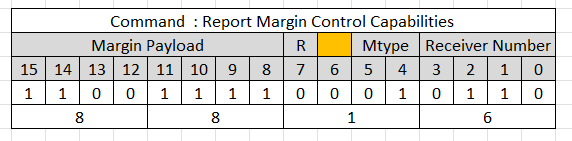
그리고 잠시 기다렸다가 해당 Lane의 Margining Lane Status Register 를 Read 합니다 .
이것이 Response인데, Margin Type 과 Receiver Nubmer 는 반드시 Command와 일치해야 합니다.
하지만 Margin Paylod는 해당 디바이스의 Margin Control Capabilities 정보를 저장해서 리턴합니다.
Host software 는 이 response를 참조하여 타겟 디바이스의 MIndErrorSampler, MSampleReportingMeshod, MIndLeftRightTiming, 그리고 MVoltageSupported 와 같은 정보를 알 수 있습니다 .
